ISSCC 2005: The CELL Microprocessor
Back to Basics
The fundamental task of a processor is to manage the flow of data through its computational units. However in the past two decades, each successive generation of processors for personal computers has added more transistors dedicated to increasing the performance of spaghetti-like integer code. For example, it is well known that typical integer codes are branchy and that branch mispredict penalties are expensive; in an effort to minimize the impact of branch instructions, transistors were used to develop highly accurate branch predictors. Aside from branch predictors, sophisticated cache hierarchies with large tag arrays and predictive cache prefetch units attempt to hide the complexity of data movement from the software, and further increase the performance of single threaded applications. The pursuit of single threaded performance can be observed in recent years in the proposal of extraordinarily deeply pipelined processors designed primarily to increase the performance of single threaded applications, at the cost of higher power consumption and larger transistor budgets.
The fundamental idea of the CELL processor project is to reverse this trend and give up the pursuit of single threaded performance, in favor of allocating additional hardware resources to perform parallel computations. That is, minimal resources are devoted toward the execution of single threaded workloads, so that multiple DSP-like processing elements can be added to perform more parallelizable multimedia-type computations. In the examination of the first implementation of the CELL processor, the theme of the shift in focus from the pursuit of single threaded integer performance to the pursuit of multiply threaded, easily parallelizable multimedia-type performance is repeated throughout.
CELL Basics
The CELL processor is a collaboration between IBM, Sony and Toshiba. The CELL processor is expected by this consortium to provide computing power an order of magnitude above and beyond what is currently available to its competitors. The International Solid-State Circuits Conference (ISSCC) 2005 was chosen by the group as the location to describe the basic hardware architecture of the processor and announce the first incarnation of the CELL processor family.
Members of the CELL processor family share basic building blocks, and depending on the requirement of the application, specific versions of the CELL processor can be quickly configured and manufactured to meet that need. The basic building blocks shared by members of the CELL family of processor are the following:
- The PowerPC Processing Element (PPE)
- The Synergistic Processing Element (SPE)
- The L2 Cache
- The internal Element Interconnect Bus(EIB)
- The shared Memory Interface Controller (MIC) and
- The FlexIO interface
Each SPE is in essence a private system-on-chip (SoC), with the processing unit connected directly to 256KB of private Load Store (LS) memory. The PPE is a dual threaded (SMT) PowerPC processor connected to the SPE's through the EIB. The PPE and SPE processing elements access system memory through the MIC, which is connected to two independent channels of Rambus XDR memory, providing 25 GB/s of memory bandwidth. The connection to I/O is done through the FlexIO interface, also provided by Rambus, providing 44.8 GB/s of raw outbound BW and 32 GB/s of raw inbound bandwidth for total I/O bandwidth of 76.8 GB/s. At ISSCC 2005, IBM announced that the first implementation of the CELL processor has been tested to operate at frequencies above 4 GHz. In the CELL processor, each SPE is capable of sustaining 4 FMADD operations per cycle. At an operating frequency of 4 GHz, the CELL processor is thus capable of achieving a peak throughput rate of 256 GFlops from the 8 SPE's. Moreover, the PPE can contribute some amount of additional compute power with its own FP and VMX units.
Processor Overview
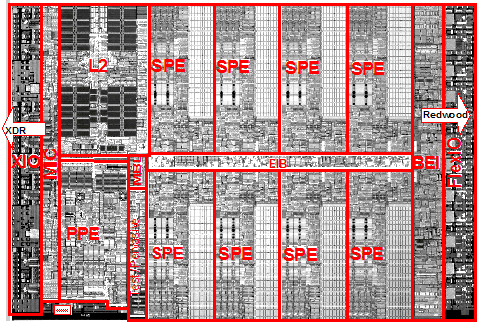
Figure 1 - Die photo of CELL processor with block diagram overlay
Figure 1 shows the die photo of the first CELL processor implementation with 8 SPE’s. The sample processor tested was able to operate at a frequency of 4 GHz with Vdd of 1.1V. The power consumption characteristics of the processor were not disclosed by IBM. However, estimates in the range of 50 to 80 Watts @ 4 GHz and 1.1 V were given. One unconfirmed report claims that at the extreme end of the frequency/voltage/power spectrum, one sample CELL processor was observed to operate at 5.6 GHz with 1.4 V Vdd and consumed 180 W of power.
As described previously, the CELL processor with 8 SPE’s operating at 4 GHz has a peak throughput rate of over 256 GFlops. To provide the proper balance between processing power and data bandwidth, an enormously capable system interconnects and memory system interface is required for the CELL processor. For that task, the CELL processor was designed as a Rambus Sandwich, with Redwood Rambus Asic Cell (RRAC) acting as the system interface on one end of the CELL processor, and the XDR (formerly Yellowstone) high bandwidth DRAM memory system interface on the other end of the CELL processor. Finally, the CELL processor has 2954 C4 contacts to the 3-2-3 organic package, and the BGA package is 42.5 mm by 42.5 mm in size. The BGA package contains 1236 contacts, 506 of which are signal interconnects and the remainder are devoted to power and ground interconnects.
Logic Depth, Circuit Design, Die Size and Process Shrink
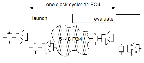
Figure 2 - Per stage circuit delay depth of 11 FO4 often left only 5~8 FO4 for logic flow
The first incarnation of the CELL processor is implemented in a 90nm SOI process. IBM claims that while the logic complexity of each pipeline stage is roughly comparable to other processors with a per stage logic depth of 20 FO4, aggressive circuit design, efficient layout and logic simplification enabled the circuit designers of the CELL processor to reduced the per stage circuit delay to 11 FO4 throughout the entire design. The design methodology deployed for the CELL processor project provides an interesting contrast to that of other IBM processor projects in that the first incarnation of the CELL processor makes use of fully custom design. Moreover, the full custom design includes the use of dynamic logic circuits in critical data paths. In the first implementation of the CELL processor, dynamic logic was deployed for both area minimization as well as performance enhancement to reach the aggressive goal of 11 FO4 circuit delay per stage. Figure 2 shows that with the circuit delay depth of 11 FO4, oftentimes only 5~8 FO4 are left for inter-latch logic flow.
The use of dynamic logic presents itself as an interesting issue in that dynamic logic circuits rely on the capability of logic transistors to retain a capacitive load as temporary storage. The decreasing capacitance and increasing leakage of each successive process generation means that dynamic logic design becomes more challenging with each successive process generation. In addition, dynamic circuits are reportedly even more challenging on SOI based process technologies. However, circuit design engineers from IBM believe that the use of dynamic logic will not present itself as an issue in the scalability of the CELL processor down to 65 nm and below. The argument was put forth that since the CELL processor is a full custom design, the task of process porting with dynamic circuits is no more and no less challenging than the task of process porting on a design without dynamic circuits. That is, since the full custom design requires the re-examination and re-optimization of transistor and circuit characteristics for each process generation, if a given set of dynamic logic circuits become impractical for specific functions at a given process node, that set of circuits can be replaced with static circuits as needed.
The process portability of the CELL processor design is an interesting topic due to the fact that the prototype CELL processor is a large device that occupies 221 mm2 of silicon area on the 90 nm process. Comparatively, the IBM PPC970FX processor has a die size of 62 mm2 on the 90 nm process. The natural question then arises as to whether Sony will choose to reduce the number of SPE’s to 4 for the version of the CELL processor to appear in the next generation Playstation, or keep the 8 SPE’s and wait for the 65 nm process before it ramps up the production of the next generation Playstation. Although no announcements or hints have been given, IBM’s belief in regards to the process portability of the CELL processor design does bode well for the 8 SPE path since process shrinks can be relied on to bring down the cost of the CELL processor at the 65 nm node and further at the 45 nm node.
Floating Point Capability
As described previously, the prototype CELL processor’s claim to fame is its ability to sustain a high throughput rate of floating point operations. The peak rating of 256 GFlops for the prototype CELL processor is unmatched by any other device announced to date. However, the SPE’s are designed for speed rather than accuracy, and the 8 floating point operations per cycle are single precision (SP) operations. Moreover, these SP operations are not fully IEEE754 compliant in terms of rounding modes. In particular, the SP FPU in the SPE rounds to zero. In this manner, the CELL processor reveals its roots in Sony's Emotion Engine. Similar to the Emotion Engine, the SPE’s single precision FPU also eschewed rounding mode trivialities for speed. Unlike the Emotion Engine, the SPE contains a double precision (DP) unit. According to IBM, the SPE’s double precision unit is fully IEEE854 compliant. This improvement represents a significant capability, as it allows the SPE to handle applications that require DP arithmetic, which was not possible for the Emotion Engine.
Naturally, nothing comes for free and the cost of computation using the DP FPU is performance. Since multiple iterations of the same FPU resources are needed for each DP computation, peak throughput of DP FP computation is substantially lower than the peak throughput of SP FP computation. The estimate given by IBM at ISSCC 2005 was that the DP FP computation in the SPE has an approximate 10:1 disadvantage in terms of throughput compared to SP FP computation. Given this estimate, the peak DP FP throughput of an 8 SPE CELL processor is approximately 25~30 GFlops when the DP FP capability of the PPE is also taken into consideration. In comparison, Earth Simulator, the machine that previously held the honor as the world’s fastest supercomputer, uses a variant of NEC’s SX-5 CPU (0.15um, 500 MHz) and achieves a rating of 8 GFlops per CPU. Clearly, the CELL processor contains enough compute power to present itself as a serious competitor not only in the multimedia-entertainment industry, but also in the scientific community that covets DP FP performance. That is, if the non-trivial challenges presented by the programming model of the CELL processor can be overcome, the CELL processor may be a serious competitor in applications that its predecessor, the Emotion Engine, could not cover.
SPE Overview
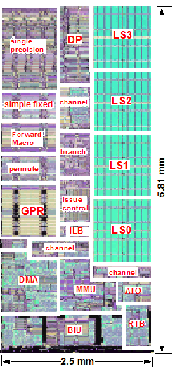
Figure 3 - SPE die photo with functional unit overlay
Figure 3 shows the die photo of the Synergistic (or just plain SIMD) Processing Element (SPE). The SPE is a specialized processing element dedicated to the computation of SIMD-type data streams. The SPE has 256KB of private memory, referred to as the Load Store (LS) unit, implemented as four separate arrays of 64 KB each. The LS is a private, non-coherent address space that is separate from the system address space. The LS is implemented using ECC protected arrays of single ported SRAM. The LS has been optimized to sustain high bandwidth and small cell size. The cell size is 0.99µm2 on the 90nm SOI process, and access latency to LS is 6 cycles.
SPE Architecture
To minimize usage of
non-computational hardware, the SPE does not have hardware for data
fetch and branch prediction. These tasks are instead relegated to
software. The SPE implements an improper subset of the VMX instruction
set, and all instructions are 32 bits in length. The SPE instructions
operate on a unified register file with 128 registers. The registers
are 128 bits in width and most instructions operate on the 128 bit
operands by treating them as four separate 32 bit operands. Due to the
18 cycle branch misprediction penalty and the lack of a branch
predictor, tremendous effort will have to be devoted to avoiding
branches. The inclusion of the large register file is thus a necessary
element in eliminating unnecessary branches via loop unrolling.
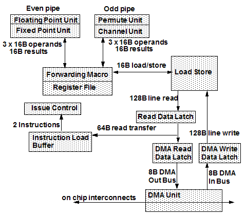
Figure 4 - SPE Organization
The SPE is an in-order processor that can issue two instructions per cycle to seven execution units in two different pipelines. Typically, each instruction makes use of 3 source operands to produce 1 result. The operands are fetched from either the register file or the forward network. Due to the in-order nature of the pipeline and the strict issue rules, the processor makes use of the forwarding network to minimize execution bubbles. To support the dual issue pipeline, each of which can source 3 operands and produce one result per cycle, the register file has 6 read ports and 2 write ports. Register file access takes 2 cycles.
Load Store Unit
The Load Store unit is a privately addressed, non-coherent address space for the SPE. Data is moved in and out of the Load Store unit in 128 Byte lines by the DMA engine. Due to the fact that the LS must simultaneously support DMA transfers into the SPE, DMA transfers out of the SPE as well as local accesses by the execution units, IBM expects that the LS unit would have a utilization rate as high as 80~90% when the SPE is running optimally. As a result, the DMA engine must schedule data transfers to avoid contentions on the system bus and LS. While the use of the software controlled data movement mechanism and the lack of a cache increases the difficulty of programming the SPE, the explicit software management aspect of the SPE means that it is well suited to support real time applications.
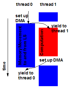
Figure 5 - Software scheduled threads overlapping computation and data streaming
In the CELL processor, the software manages the DMA and reserves channels to move data to and from the LS. The DMA is programmed and resources allocated for the movement of data in response to requests. The request queue in the SPE supports up to 16 outstanding requests. Each request can transfer up to 16 Kb of data. Once the data is moved into the LS, the SPE then performs the computation by accessing the private LS in isolation. Ideally, each SPE would overlap computation with data streaming, and two or more software managed threads can operate concurrently on a SPE at a given instance in time. In such a scenario, while one thread is moving data in and out of the LS via the DMA engine, a second thread can occupy the computing resources of the SPE. Figure 5 illustrates the basic idea of using software managed threads to explicitly overlap computation and data movement.
SPE Pipeline
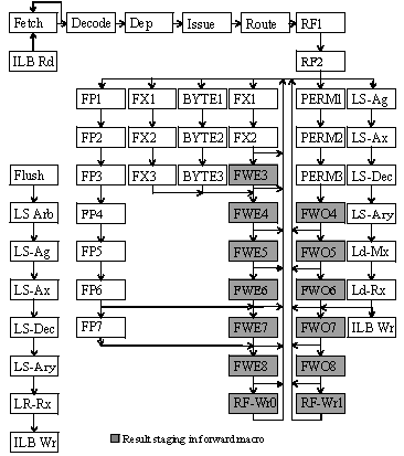
Figure 6 - SPE pipeline diagram
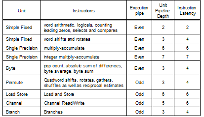
Table 1 - Unit latencies for SPE instructions.
Figure 6 shows the pipeline diagram of the SPE and Table 1 shows the unit latency of the SPE. Figure 6 shows that the SPE pipeline makes heavy use of the forward-and-delay concept to avoid the access latency of a register file access in the case of dependent instructions that flow through the pipeline in rapid succession.
One interesting aspect of the floating point pipeline is that the same arrays are used for floating point computation as well as integer multiplication. As a result, integer multiplies are sent to the floating point pipeline, and the floating point pipeline bypasses the FP handling and computes the integer multiply.
SPE Schmoo Plot
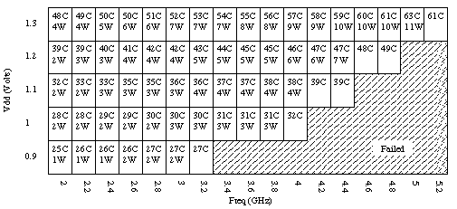
Figure 7 - Schmoo plot for the SPE
Figure 7 shows the schmoo plot for the SPE. The schmoo plot shows that the SPE can comfortably operate at a frequency of 4 GHz with Vdd of 1.1 V, consuming approximately 4 W. The schmoo plot also reveals that due to the careful segmentation of signal path lengths, the design is far from being wire delay limited. Frequency scaling relative to voltage continues past 1.3 V. This schmoo plot also contributes to the plausibility of the unconfirmed report that the CELL processor could operate at upwards of 5.6 GHz.
“Unknown” Functional Units: ATO and RTB
Oftentimes when a paper relating to a complex project is written collaboratively by a group of people, details are lost. Still, it appeared as rather humorous that of the six design engineers and architects from the CELL processor project present at Tuesday evening’s chat session, no one could recall what the acronyms ATO and RTB stood for. ATO and RTB are functional blocks labeled in the floorplan of the SPE. However, the functionality of these functional blocks or the meaning of the acronym were neither noted on the floorplan, nor explained in the paper, nor mentioned in the technical presentation. In an effort to cover all the corners, this author placed the question on a list of questions to be asked of the CELL project team members. Hilarity thus ensued as slightly embarrassed CELL project members stared blankly at each other in an attempt to recall the functionality or definition of the acronyms.
In all fairness, since the SPE was presented on Monday and the CELL processor itself was presented on Tuesday, CELL project members responsible for the SPE were not present for Tuesday evening’s chat sessions. As a result, the team members responsible for the overall CELL processor and internal system interconnects were asked to recall the meaning of acronyms of internal functional units within the SPE. Hence, the task was unnecessarily complicated by the absence of key personnel that would have been able to provide the answer faster than the CELL processor can rotate a million triangles by 12 degrees about the Z axis.
After some discussion (and more wine), it was determined that the ATO unit is most likely the Atomic (memory) unit responsible for coherency observation/interaction with dataflow on the EIB. Then, after the injection of more liquid refreshments (CH3CH2OH), it was theorized that the RTB most likely stood for some sort of Register Translation Block whose precise functionality was unknown to those outside of the SPE. However, this theory would turn out to be incorrect.
Finally, after sufficient numbers of hydrocarbon bonds have been broken down into H-OH on Wednesday, a member of the CELL processor team member tracked down the relevant information and he writes:
The R in RTB is an internal 1 character identifier that denotes that the RTB block is a unit in the SPE. The TB in RTB stands for "Test Block". It contains the ABIST (Array Built In Self Test) engines for the Local Store and other arrays in the SPE, as well as other test related control functions for the SPE.
Element Interconnect Bus
The element interconnect bus is the on chip interconnect that ties together all of the processing, memory, and I/O elements on the CELL processor. The EIB is implemented as a set of four concentric rings that is routed through portions of the SPE, where each ring is a 128 bit wide interconnect. To reduce coupling noises, the wires are arranged in groups of four and interleaved with ground and power shields. To further reduce coupling noises, the direction of data flow alternates between each adjacent ring pair. Data travels on the EIB through staged buffer/repeaters at the boundaries of each SPE. That is, data is driven by one set of staged buffer and latched by the buffer at the next stage every clock cycle. Data moving from one SPE through other SPE’s requires the use of repeaters in the intermediary SPE’s for the duration of the transfer. Independently from the buffer/repeater elements, separate data on/off ramps exist in the BIU of the SPE, as data targeted for the LS unit of a given SPE can be off-loaded at the BIU. Similarly, outgoing data can be placed onto the EIB by the BIU.
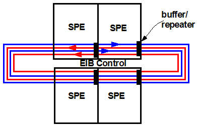
Figure 8 - Counter rotational rings of the EIB - 4 SPE’s shown
The design of the EIB is specifically geared toward the scalability of the CELL processor. That is, signal path lengths on the EIB do not change regardless of the number of SPE’s in a given CELL processor configuration. Since the data travels no more than the width of one SPE, more SPE’s on a given CELL processor simply means that the data transport latency increases by the number of additional hops through those SPE’s. Data transfer through the EIB is controlled by the EIB controller, and the EIB controller works with the DMA engine and the channel controllers to reserve the buffers drivers for certain number of cycles for each data transfer request. The data transfer algorithm works by reserving channel capacity for each data transfer, thus providing support for real time applications. Finally, the design and implementation of the EIB has a curious side effect in that it limits the current version of the CELL processor to expand only along the horizontal axis. Thus, the EIB enables the CELL processor to be highly configurable and SPE’s can be quickly and easily added or removed along the horizontal axis, and the maximum number of SPE’s that can be added is set by the maximum width of the chip allowable by the reticule size of the fabrication equipment.
The POWERPC Processing Element
Neither microarchitectural details nor the performance characteristics of the POWERPC Processing Element were disclosed by IBM during ISSCC 2005. However, what is known is that the PPE processor core is a new core that is fully compliant with the POWERPC instruction set, the VMX instruction set extension inclusive. Additionally, the PPE core is described as a two issue, in-order, 64 bit processor that supports 2 way SMT. The L1 cache sizes of the PPE is reported to be 32KB each, and the unified L2 cache is 512 KB in size. Furthermore, the lineage of the PPE can be traced to a research project commissioned by IBM to examine high speed processor design with aggressive circuit implementations. The results of this research project were published by IBM first in the Journal of Solid State Circuits (JSSC) in 1998, then again in ISSCC 2000.
The paper published in JSSC in 1998 described a processor implementation that supported a subset of the POWERPC instruction set, and the paper published in ISSCC 2000 described a processor that supported the complete POWERPC instruction set and operated at 1 GHz on a 0.25µm process technology. The microarchitecture of the research processor was disclosed in some detail in the ISSCC 2000 paper. However, that processor was a single issue processor whose design goal was to reach high operating frequency by limiting pipestage delay to 13 FO4, and power consumption limitations were not considered. For the PPE, several major changes in the design goal dictated changes in the microarchitecture from the research processor disclosed at ISSCC in 2000. Firstly, to further increase frequency, the per stage circuit delay design target was lowered from 13 FO4 to 11 FO4. Secondly, limiting power consumption and minimize leakage current were added as high priority design goals for the PPE. Collectively, these changes limited the per stage logic depth, and the pipeline was lengthened as a result. The addition of SMT and the two issue design goal completed the metamorphosis of the research processor to the PPE. The result is a processing core that operates at a high frequency with relatively low power consumption, and perhaps relatively poorer scalar performance compared to the beefy POWER5 processor core.
Rambus XDR Memory System
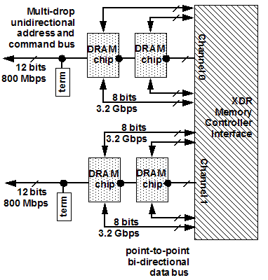
Figure 9 - The two channel XDR Memory System
To provide machine balance and support the peak rating of more than 256 SP GFlops (or 25~30 DP GFlops), the CELL processor requires an enormously capable memory system. For that purpose, two channels of Rambus XDR memory is used to obtain 25.2 GB/s of memory bandwidth.
In the XDR memory system, each channel can support a maximum of thirty-six devices connected to the same command and address bus. The data bus of each device connects to the memory controller through a set of bi-directional point-to-point connections. In the XDR memory system, address and command are sent on the address and command bus at a rate of 800 Mbits per second (Mbps), and the point to point interface operates at a datarate of 3.2 Gbps. Using DRAM devices with 16 bit wide data busses, each channel of XDR memory can sustain a maximum bandwidth of 102.4 Gbps (2 x 16 x 3.2), or 12.6 GB/s. The CELL processor can thus achieve a maximum bandwidth of 25.2 GB/s with a 2 channel, 4 device configuration.
The obvious advantage of the XDR memory system is the bandwidth that it provides to the CELL processor. However, in the configuration illustrated in figure 9, the maximum of 4 DRAM devices means that the CELL processor is limited to 256 MB of memory, given that the highest capacity XDR DRAM device is currently 512 Mbits. Fortunately, XDR DRAM devices could in theory be reconfigured in such a way so that upwards of 36 XDR devices can be connected to the same 36 bit wide channel and provide 1 bit wide data bus each to the 36 bit wide point-to-point interconnect. In such a configuration, a two channel XDR memory can support upwards of 16 GB of ECC protected memory with 256 Mbit DRAM devices or 32 GB of ECC protected memory with 512 Mbit DRAM devices. As a result, the CELL processor could in theory address a large amount of memory if the price premium of XDR DRAM devices can be minimized. One intriguing note reported by Dave Bursky of Electronic Design Magazine is that the XDR memory system makes use of 72 pairs of differential signals for the data bus. The figure seventy-two implies that the CELL processor does indeed support ECC. Since ECC support is clearly not a requirement of a processor to be used in a game machine, the presence of ECC support, if confirmed, would clearly indicate IBM’s ambition to promote the use of CELL processors for serious computational applications outside of the application domain of the Sony Playstation.
Incidentally, Toshiba is a manufacturer of XDR DRAM devices. Presumably it brought the XDR memory controller and memory system design expertise to the table, and could ramp up production of XDR DRAM devices as needed.
FlexIO System Interface
At ISSCC 2005, Rambus
presented a paper on the FlexIO interface used on the CELL processor.
However, the presentation was limited to describing the physical layer
interconnect. Specifically, the difficulties of implementing the
Redwood Rambus ASIC Cell on IBM’s 90nm SOI process were examined in
some detail. While circuit level issues regarding the challenges of
designing high speed I/O interfaces on an SOI based process are in
their own right extremely intriguing topics, the focus of this article
is geared toward the architectural implications of the high bandwidth
interface. As a result, the circuit level details will not be covered
here. Interested readers are encouraged to seek out details on Rambus’s
Redwood technology separately.
What is known about the system interface of the CELL processor is that the FlexIO consists of 12 byte lanes. Each byte lane is a set of 8 bit wide, source synchronous, unidirectional, point-to-point interconnects. The FlexIO makes use of 96 differential signaling pairs to achieve the data rate of 6.4 Gb per second per signal pair, and that data rate in turn translates to 6.4 GB/s per byte lane. The 12 byte lanes are asymmetric in configuration. That is, 7 byte lanes are outbound from the CELL processor, while 5 byte lanes are inbound to the CELL processor. The 12 byte lanes thus provide 44.8 GB/s of raw outbound bandwidth and 32 GB/s of raw inbound bandwidth for total I/O bandwidth of 76.8 GB/s. Furthermore, the byte lanes are arranged into two groups of ports: one group of ports are dedicated to non-coherent off-chip traffic, while the other group of ports are usable for coherent off-chip traffic. It seems clear that Sony itself is unlikely to make use of a coherent, multiple CELL processor configuration for Playstation 3. However, the fact that the PPE and the SPE’s can snoop traffic transported through the EIB, and that coherency traffic can be sent to other CELL processors via a coherent interface, means that the CELL processor can indeed be an interesting processor. If nothing else, the CELL processor should enable startups that propose to build FlexIO based coherency switches to garner immediate interest from venture capitalists.
Summary
The CELL processor presents an intriguing alternative in its pursuit of performance. It seems to be a forgone conclusion that the CELL processor will be an enormously successful product, and that millions of CELL processors will be sold as the processors that power the next generation Sony Playstation. However, IBM has designed some features into the CELL processor that clearly reveals its ambition in seeking new applications for the CELL processor. At ISSCC 2005, much fanfare has been generated by the rating of 256 GFlops @ 4 GHz for the CELL processor. However, it is the little mentioned double precision capability and the yet undisclosed system level coherency mechanism that appear to be the most intriguing aspects that could enable the CELL processor to find success not just inside the Playstation, but outside of it as well.
References
[1] J. Silberman et. al., “A 1.0- GHz Single-Issue 64-Bit PowerPC
Integer Processor”, IEEE Journal of Solid-State Circuits, Vol 33,
No.11, Nov 1998.
[2] P. Hofstee et. al., “A 1 GHz Single-Issue 64b PowerPC Processor”,
International Solid-State Circuits Conference Technical Digest, Feb.
2000.
[3] N. Rohrer et. al. “PowerPC in 130nm and 90nm Technologies”,
International Solid-State Circuits Conference Technical Digest, Feb.
2004.
[4] B. Flachs et. al. “A Streaming Processing Unit for A CELL
Processor”, International Solid-State Circuits Conference Technical
Digest, Feb. 2005.
[5] D. Pham et. al. “The Design and Implementation of a
First-Generation CELL Processor”, International Solid-State Circuits
Conference Technical Digest, Feb. 2005.
[6] J. Kuang et. al. “A Double-Precision Multiplier with Fine-Grained
Clock-Gating Support for a First-Generation CELL Processor”,
International Solid-State Circuits Conference Technical Digest, Feb.
2005.
[7] S. Dhong et. al. “A 4.8 GHz Fully Pipelined Embedded SRAM in the
Streaming Processor of a CELL Processor”, International Solid-State
Circuits Conference Technical Digest, Feb. 2005.
[8] K. Chang et. al. “Clocking and Circuit Design for a Parallel I/O on
a First-Generation CELL Processor”, International Solid-State Circuits
Conference Technical Digest, Feb. 2005.
Copyright 2005 David T. Wang. All rights reserved. No portion of this article, in part or whole, may be reproduced, copied, transmitted, stored, downloaded, in any manner in anyway for any purpose whatsoever without the express written consent from the author.